In this article, you will learn how to assemble printed circuit boards (PCBs) with surface mount technology (SMT) components in a production environment. Surface Mount Technology (SMT) became the technology of choice for Printed Circuit Board Assembly (PCBA) in the early 1980’s as electronic products became smaller and demanded smarter, easier to use and more accurate technology.
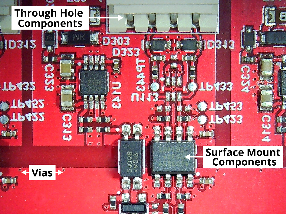
Prior to the popularity of SMT, through-hole technology was the dominant technology where component leads (axial or radial style) were inserted into holes on a bare PCB and then soldered. One side of the board was referred to as the “component side” and the other side as the “solder side”, a term that is still used today.
Even today, both technologies are still in use and can even coexist on the same board, each with its own advantages. Because through-hole technology allows for a stronger physical connection, it is considered a better way to design highly reliable products for rugged or commercial applications that need to withstand environmental stress.
It is also a good choice for components that may be subjected to mechanical stress (i.e., vibration) due to mass (e.g., connectors) or for larger components (e.g., decoupling capacitors, transformers, etc.).
Surface mount technology, originally known as planar mount, is a method of mounting electronic components to the surface of a printed circuit board using flat leads or small metal pads. This technique is helpful when large quantities of PCBs are required or when miniaturization is needed to meet unique requirements.
Unlike through-hole technology, which allows components to be easily mounted on either side of the board within limits, SMT technology does not require through-holes to create connections between board layers.
Today’s multilayer SMT PCB stacks range from 2 to 32 layers, with 4 and 6 layers being the most common. In this case, the advantage of surface mount technology is to further reduce the size of the PCB by increasing the number of connections per square inch of PCB. To better understand the complexity, let’s take a look inside a PCB stack.
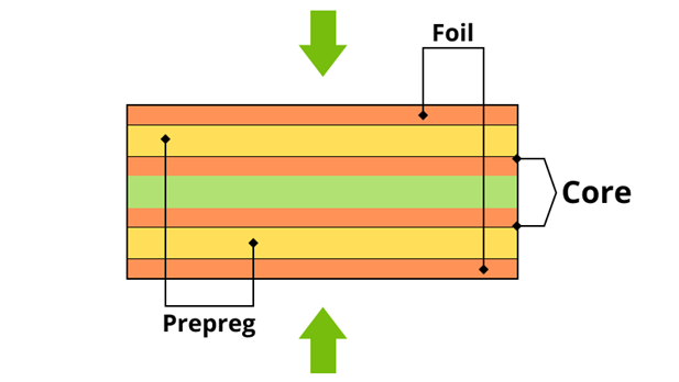
Note that the PCB in Figure 2 consists of several layers. This arrangement of materials is called a “PCB stack” and can vary depending on the PCB requirements.
The two key components of the stack are the copper-clad layers (for electrical conductivity) and the laminating layers (to provide structure and insulation).
The copper-clad layers are “etched” to create a specific wiring pattern and can vary in thickness: thicker layers allow more current to flow.
The standard copper thickness used is 1 ounce. Interestingly, copper thickness in PCB manufacturing is measured in ounces (oz.), which is a specific weight of copper spread over an area of 1 square foot (a thickness equal to 1.37 mils or 0.0348 mm).
In addition, 1.5 oz. and 2 oz. are also standard copper thicknesses, which will allow correspondingly higher currents to flow in a circuit. The laminates consist of fiber-reinforced epoxy resins. They are available in two basic types: “Cores”, with a pre-cured copper foil, and “PrePreg”, without a copper foil and without the epoxy fully cured.
The PrePreg layer acts as the glue that holds all the layers together as they are assembled and cured by pressure and heat.
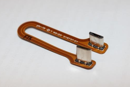
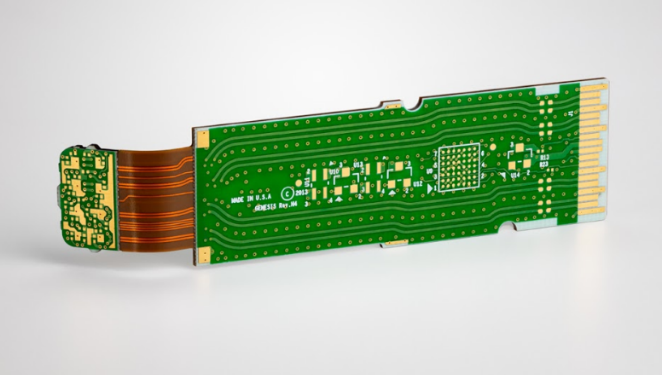
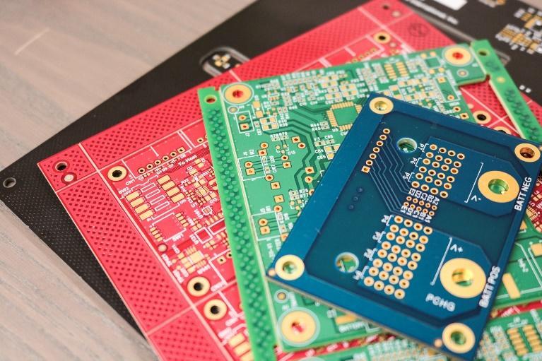
The most common type of laminate used in PCB manufacturing is called “FR4”, but different laminates (BT Epoxy, Polyimide, Teflon, etc.) can be used for more demanding applications such as high frequency or high temperature. Also, there are different types of PCBs: rigid, flexible and rigid-flexible. Rigid PCBs are more traditional PCBs and, as the name suggests, are inherently rigid or inflexible.
Flexible PCBs are built by replacing the core or prepreg layer with a thin polyimide layer that can be bent or shaped to fit space constraint requirements. Flexible PCBs are becoming more mainstream today due to the miniaturization and popularity of wearable devices. On the other hand, rigid-flex PCBs are a combination of rigid and flexible PCBs, combining the versatility of flexible circuits with the stability of rigid PCBs. By eliminating the need for connectors and cables, the reliability of board-to-board connections is improved, resulting in a more reliable system. It is the most expensive type of PCB and is primarily used in aerospace or military applications.
In addition, laminates are available in a variety of thicknesses to accommodate a wide range of stacking configurations, PCB thicknesses, and PCB types. Standard options for total thickness of all laminates on a rigid PCB range from 0.2 mm to 3.2 mm (0.008 in. to 0.240 in.). The most common options include 0.8 mm (0.032 in.), 1.6 mm (0.063 in.), and 3.175 mm (0.125 in.).
While common boards fall within this range, backsheets tend to be thicker, approaching the upper end of the range for added mechanical strength. On the other hand, we have very thin (0.065 mm to 0.42 mm) and highly flexible PCBs. PCBs usually have their outer copper layer covered in a thin “soldermask” to protect the copper from corrosion and act as an insulator, exposing only the pads. In most cases, the soldermask is green, but it can also be red, blue, black, white, etc. On top of the soldermask, the PCB is covered with a thin layer of copper.
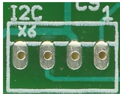
Over the soldermask, the PCB presents a layer of inscription called a silkscreen.
A silkscreen is a layer of ink traces used to mark text and symbols on the PCB to identify the location of components (based on reference indicators) and to specify the orientation of components.
A word of caution: It is important to avoid overlapping silkscreens on pads, as shown in Figure 6, as they can create problems during the soldering process, which can be disastrous in the long run.
The most common finishes for pads in use today are: Hot Air Solder Leveling (HASL), Lead Free HASL, Immersion Silver (Ag), Immersion Tin (Sn), Electroless Nickel Immersion Gold (ENIG) and Electroless Nickel Palladium Immersion Gold (ENEPIG). These technologies are listed from least to most expensive.
Simply put, a better surface finish provides a flatter surface for the pads, allowing for better soldering of the components on the pads.
ENIG is a proven industry standard that is easily implemented by most PCB manufacturers, and ENIG deposits provide a tighter, more uniform grain structure, maintain high solderability, and resist corrosion.
The most commonly used stack today is a 4-layer stack with ENIG coating and green soldermask, with two middle layers dedicated to “power” (VCC or a combination of VCC values) and “ground” (GND).
The remaining outer layers are used for connections between components.
Now that we have a general understanding of PCB technology, let’s review the various steps involved in the PCB assembly process.
Pre-PCB Assembly
Printed Circuit Board Design
Electronic designers translate functional requirements into “schematics” – symbolic recipes that show which electronic components will be used and how they will be connected to form a functional circuit.
The schematic is abstracted to contain conceptual information about the circuit. The schematic “recipe” is then transformed into a “PCB layout” – a set of drawings showing the physical location of the electronic components and their connections in a way that can be manufactured.
The layout includes a 2D drawing of each copper layer, drilling (through-hole) information, stacking information, quality requirements, and a 3D model of the final board.
Designers use computer-aided design (CAD) software to enforce design rules and perform automated checks to ensure that the final result matches the specifications of the schematic and meets manufacturing requirements.
CAD software is used to convert the design into the files required by the board manufacturer (Gerber files) and the assembly house (pick-and-place files and/or assembly files).
Following this, a validation process (design rule check) is performed to determine if there are any layout errors that could affect board functionality or manufacturability.
The design is checked for quality, accuracy, modularity and consistency through DFM (Design for Manufacturing) and DFA (Design for Assembly).
PCB Manufacturing
Upon completion of design verification, manufacturing files are prepared that contain information in styles and formats generally accepted by PCB manufacturers.
Manufacturing files include format-specific Gerber files, net lists, fabrication drawings, assembly drawings, NC drill files, blind/buried hole information, bills of materials, and PCB panel diagrams.
Prepare PCBAs and Components
Once the PCBAs have been fabricated and the components have been purchased, they need to be prepared for assembly.
One of the preparation steps for reflow assembly is to ensure that the PCBA and components have low humidity.
PCBs and moisture sensitive components must be baked to dry prior to assembly.
PCBA and component baking is a process that takes place in a temperature controlled oven, where the baking temperature and time depends on the thickness and exposure of the PCB and components (Standard J-STD-033).
Typical baking temperatures range from 125 degrees Celsius to 150 degrees Celsius and can last up to 24 hours. PCB Baking avoids problems such as IC popping and PCB delamination that can occur when moisture is present on the board.
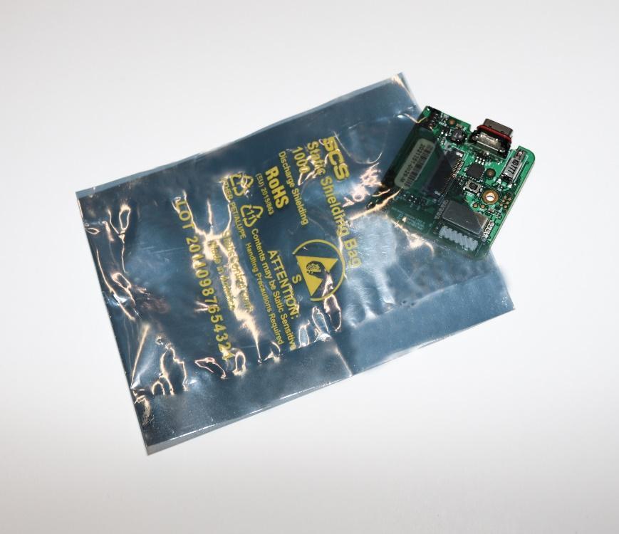
Moisture sensitive parts must be vacuum sealed in a moisture proof bag (Figure 7) with desiccant (Figure 9) and a humidity indicator card (Figure 10) and can only be removed from the bag prior to assembly.
After removal, there is a 168-hour window to perform the reflow process (for MSL3 components). After this time, the assembly must be rebaked for assembly or storage purposes.
Preparing the PCB for Assembly
Prior to assembly, a number of preparations need to be completed to ensure a successful production run.
Based on the manufacturing documentation, the engineer must prepare the work instructions, define the program and create a data log.
In the case of screen printing, preparing the stencil is an important step. As the term implies, stencils are sheets of material with holes that correspond to component pads on the PCB.
Each PCB requires a unique stencil, and this method of solder paste application is particularly useful in high-volume production. I will discuss this more in the next section.
Next, a machine program must be prepared for each product. Programming is done based on mounting position information, PCB length, width and thickness, material information, etc.
One option is to do this preparation off-line while the line is processing the previous run. The machine program is set offline so that the next run can be loaded quickly without wasting time.
In the case of special applications, prerequisites need to be determined and planned in advance.
For example, for flexible PCBs it is important to consider the use of an SMT tray, which helps to support and transport the flexible PCB through the SMT process.
PCB Assembly
Solder Paste Application
Manufactured circuit boards are initially assembled by applying solder paste to specified pads.
Solder paste is a combination of metallic solder particles and flux that helps clean the soldered surface of impurities and oxidation. It is also used as an adhesive to bond electronic components to the printed circuit board.
Solder paste application can be accomplished by stencil screen printing of solder paste or by more advanced non-contact jet printing methods. Once applied, the stencil must be cleaned and used for the next board.
For each new design, a new stencil must be manufactured, which can be very expensive, especially at low to medium production levels.
Jet printing, on the other hand, is a non-contact method that deposits the exact amount of solder on each surface mount pad and allows solder to be applied to approximately 40,000 pads per hour, with dispensing speeds in excess of 1 million dots per hour.
The technology increases solder paste volume by applying individual dots to achieve the correct amount for each component.
Jet printing is better suited for specialized applications such as pin-in-paste, paste-in-cavity, etc., where the 3D features of the PCBA cannot be served by 2D technology (stencil application).
Although jet printing has gained a lot of momentum due to the inherent advantages it offers, such as faster changeovers and no need for stencils, stencil-based screen printing is still the preferred method for solder paste application in high-volume production situations.
For designs with a mix of large and very small components, applying the right amount of solder in one setup can be a challenge, and screen printing combined with jet printing is an ideal solution.
After applying solder paste, special considerations must be made for heavier components. Typically, heavier components will be soldered in the second pass of the reflow process.
However, if they end up on the bottom of the board and require a second pass through the oven, they must be tacked in place to avoid shifting due to gravity.
To accomplish this, add drops of SMT adhesive based on the location of the larger components (manual/automatic) before the components are placed.
Solder Paste Inspection
After applying solder paste by either method, and for high volume requirements, perform a solder paste inspection (SPI) to ensure alignment, quantity, and quality of solder paste deposits.
Incorrect solder paste printing can lead to defective solder joints, resulting in scrap. Too much solder paste can lead to short circuits and bridging, while not enough solder paste will not create the required electrical connection.
Picking and Placing Components
After applying solder paste, the next step is to place the component on the solder joint.
For SMT technology, this process is handled by pick-and-place machines that place a variety of electronic components such as capacitors, resistors, ICs, etc. at high speeds and with high precision.
Surface mount components are supplied to the machine in the form of reels or trays that are loaded onto a feeder mounted on the pick and place machine.
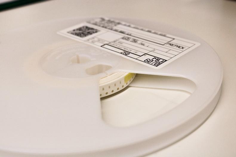
Based on the PCB design file, the pick-and-place machine will pick up each component (with pre-programmed XY coordinates and rotation) from the tray or reel using vacuum hoses, pneumatic suction cups, or fixtures, and carefully place it at the precise location on the board where the solder paste will be applied.
Today’s fastest placement machines offer placement speeds of up to 250,000 CPH (components per hour), which can be achieved by optimizing the combination of several PnP machines.
Component placement accuracy, integrity, orientation and polarity are checked at this stage.
Reflow Soldering
Once the components are in place, they must be soldered to securely attach to the contact pads. During this process, the PCB is moved into a reflow oven where the solder paste melts and bonds the components and contacts at high temperatures to form a solder joint.
It has become common practice for miniaturized PCBAs to use a nitrogen inerting atmosphere during the soldering process. Nitrogen-based reflow environments minimize the chance of oxidation on the soldering surface.
Longer reflow ovens will have more temperature zones, which will allow for smoother temperature transitions between zones, thus reproducing the recommended solder profile and yielding better results.
Standard reflow ovens have four temperature zones (see diagram below):
Preheat Zone: The solder paste is activated at this temperature.
Absorption/Heat Soak Zone: The temperature of the various components is stabilized at this temperature.
Reflow zone: This zone has the highest temperature and is when the solder paste is completely melted. The time in this zone should be shorter, otherwise the PCB/components may be damaged.
Cooling Zone: The temperature cools below the solidification point of the solder paste, allowing the solder joint to solidify.
Temperatures in these areas must always be controlled within appropriate limits to avoid damaging components and compromising solder quality.
It is important to note that today, due to the negative environmental and health impacts of leaded solder, almost all leaded solder will be phased out and RoHS compliant lead-free solder will be more commonly used.
This step completes the PCB assembly process.
Post-PCBA Quality Control
Manual Inspection
Although not the most reliable inspection method, we mention it here because the board needs to be manually inspected by a PCBA technician at each step of the assembly process.
This is especially true for boards with low component density and can be challenging for advanced SMT boards.
Automated Optical Inspection
The AOI method uses multiple high-resolution cameras mounted at different angles to detect board defects and soldering flaws.AOI imaging technology has evolved from 2D, which is used for simple inspection, measurement, or orientation detection, to 3D imaging, which provides accurate data.
This inspection method can detect board defects such as wrong/missing parts, incorrect orientation and polarity, and tilted (known in the industry as tombstoning) or flipped components.
It can also detect solder defects such as no/insufficient solder, too much solder, or solder bridges.
Although 3D imaging is popular, AOI systems are more efficient when using both 2D and 3D inspection techniques.
X-Ray Inspection
X-Ray inspection is typically used to test the quality and accuracy of PCB soldering on complex, high-density chips where optical inspection cannot be applied.
When applied, X-rays determine the accuracy of the solder and can detect defects hidden under the IC package.
Defects detected include excessive solder (e.g., solder buildup, bridging), open solder joints, pin warpage, and misaligned joints.
It is the inspection method of choice for high-density assemblies such as BGAs because the technique allows you to see “inside” the PCB assembly.
Testing
After PCB assembly, the final PCB should be tested by a QC engineer to identify any problems or defects.
There are two main types of testing, flying probe testing and test fixturing. Flying probe is the preferred test method for low volume, critical application PCBAs (military, transportation, aerospace).
The test involves the use of multiple electrical probes that are automatically contacted and applied to the board. Some probes provide external stimuli and some read the board’s response.
Planning the test, programming the machine and executing the test is a process that requires a great deal of engineering input. Flying probe machines are usually very expensive and are often preferred for testing PCBAs for critical applications.
For volume production, test fixtures are a better choice. They are dedicated or customized test platforms for unique PCBAs. Using static probes, electrical signals and power are applied to the PCB and the output is inspected and measured.
This test will ensure that the PCB meets the electrical requirements specified in the design. The test may take a few seconds to a few minutes.
In addition to testing, final production firmware can also be loaded onto the board at this stage.
Preparation
After testing, the board is cleaned using an ultrasonic cleaning method designed to wash away any flux, resin or solder residue, dust or dirt that may have accumulated during assembly.
After cleaning, the board is ready for conformal coating, where a thin layer of protective coating material is applied to the board to protect it from moisture contamination, corrosion, oxidation, etc. The coating is applied to the board to prevent it from being contaminated by moisture.
It protects the PCB from mechanical vibration, thermal shock, and other adverse environmental conditions.
Finally, the PCBA is now ready to be packaged and shipped. pCBAs are usually packaged in anti-static bags.
Assembly Design
It would be unwise to end this blog without mentioning the principles of assembly design.
We know the importance of designing with a vision for manufacturing, assembly, cost, reliability, testability, serviceability, supply chain, regulatory compliance, innovation, recyclability, and more.
With PCBAs, if the initial PCBA design focuses on the board without considering the application, use case, or system environment, the PCBA will not fulfill the requirements of the assembly design.
On its own, a PCBA design may be perfect, but there are other issues to consider – are there components available for production orders, what are the sizes and quantities of the components being used, and are they suitable for high-volume production?
The primary goal of Design for Assembly (DFA) is to eliminate complexity and reduce uncertainty while increasing efficiency.
With this principle in mind, designers are encouraged to look at the big picture and consider the impact of the design at every stage.
The PCBA design decisions made by the designer will not only affect the assembly of the PCBA, but will also have a direct impact on the form, quality, and reliability of the finished product.