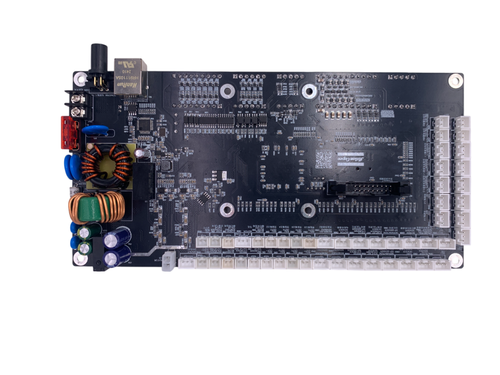
In daily PCB design, we encounter various safety spacing challenges, such as the spacing between vias and pads, traces and traces, etc. These spacing requirements should be carefully considered.

We categorize these spacing requirements into two types:
- Electrical Safety Spacing
- Non-Electrical Safety Spacing
Electrical Safety Spacing
- Trace-to-Trace Spacing
- This spacing depends on the PCB manufacturer’s capabilities.
- Recommended minimum: 2 mil (trace-to-trace or trace-to-pad).
- From a manufacturing perspective, larger spacing is preferred when possible.
- A common standard spacing is 10 mil.
- Hole Diameter & Pad Width
- Mechanical drilling: Minimum hole diameter ≥ 0.2mm.
- Laser drilling: Recommended minimum ≥ 2 mil.
- Hole diameter tolerance varies slightly by material but is generally controlled within 0.05mm.
- Minimum pad width ≥ 0.2mm.
- Pad-to-Pad Spacing
- Recommended minimum spacing: 0.2mm (subject to PCB manufacturer’s capability).
- Copper-to-Board Edge Spacing
- Minimum spacing between copper pours and board edge: 0.3mm.
- For large-area copper pours, a 50mil (1.27mm) setback from the board edge is typically applied.
- Reasoning: Prevents potential issues such as copper exposure, warping, or electrical shorts.
- Implementation:
- Draw a keepout layer at the board edge.
- Set the copper pour spacing relative to the keepout layer.
Non-Electrical Safety Spacing
- Silkscreen Text Width, Height & Spacing
- Standard values: 5/30 mil (width/height) or 6/36 mil.
- Why? Excessively small text may appear blurred after printing.
- Silkscreen-to-Pad Spacing
- General rule: Silkscreen must not overlap pads (prevents solderability issues).
- Recommended spacing: 8 mil (minimum acceptable: 2 mil for dense designs).
- Manufacturer adjustment: If silkscreen accidentally overlaps pads, manufacturers will automatically remove the overlapping portion to ensure proper soldering.
- 3D Mechanical Height & Horizontal Spacing
- Component placement: Must avoid conflicts with mechanical structures (both horizontally and vertically).
- Design considerations:
- Spacing between components.
- Compatibility between assembled PCB and enclosure.
- Reserve safety spacing for all critical interfaces.


