Introduction
Hardware development is the process of turning an idea into a real electronic product — from a simple desk lamp to a sophisticated aerospace control system.
Let’s explore how a hardware product evolves from concept to a fully functional prototype.
1. System Architecture Analysis
The first step is to analyze the overall system architecture.
This involves:
- Defining the product’s key functions and design goals;
- Breaking down the system into functional modules (power, controller, communication, sensors, etc.);
- Checking for redundancy or conflicts among modules.
A well-structured system architecture ensures a smooth development process.
2. Component Selection
Once the architecture is finalized, engineers move to component selection — one of the most critical stages.
Key considerations include:
- Choosing core ICs and key modules that meet functional requirements;
- Evaluating stability, temperature tolerance, and supply chain availability;
- Ensuring long-term component sourcing to avoid obsolescence issues.
Proper component selection directly affects performance, cost, and product lifespan.
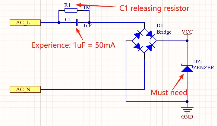
3. Schematic Design
At this stage, engineers design the schematic diagram, defining how every component connects electrically.
This includes:
- Power circuit design for voltage stability;
- Signal routing and noise management;
- Parameter calculation for resistors, capacitors, and ICs;
- Cross-referencing component datasheets for proper integration.
Simulation tools are often used alongside schematics to verify circuit behavior.
4. PCB Design
PCB (Printed Circuit Board) design translates the schematic into a real, manufacturable circuit board.
This process requires attention to:
- Logical component placement based on power and signal flow;
- Proper trace width, impedance control, and grounding;
- Minimizing crosstalk and ensuring electromagnetic compatibility;
- A balance between functionality, aesthetics, and manufacturability.
High-quality PCB design ensures signal integrity and product reliability.
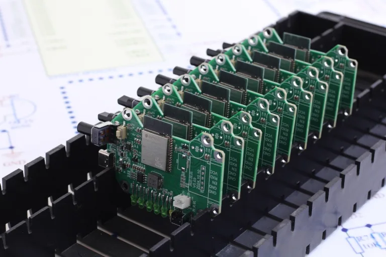
5. Prototyping and Assembly
After PCB design, the prototype board is fabricated.
- Reliable PCB manufacturers are selected to guarantee quality;
- Components are manually or automatically soldered;
- The assembled board is inspected for shorts, opens, and soldering defects.
This step results in a working hardware prototype ready for firmware integration.
6. Firmware Programming
Once assembly is complete, the firmware — the embedded software — is programmed into the controller chip.
Depending on workflow, this can be handled by embedded engineers or by the hardware team itself.
After programming, the board’s functions can be tested and validated.
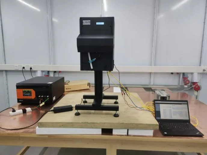
7. Testing and Validation
The final step is comprehensive testing, including:
- Functional testing
- Signal integrity and noise validation
- Performance and stability evaluation
If you are looking for a reliable and experienced hardware development team, Tronixv offers end-to-end services from system architecture and PCB design to firmware development and prototype testing — contact us and let’s turn your product ideas into reality.