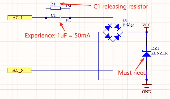
In electronic design, engineers use a schematic diagram to plan and analyze circuits. A schematic shows symbols for components and the lines that connect them, but it is purely conceptual — it cannot make a motor spin, light an LED, or perform any physical function.
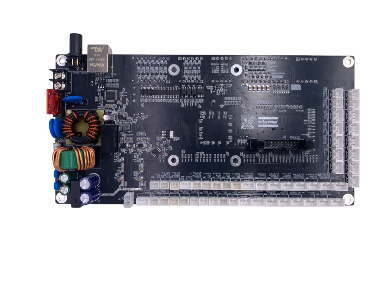
To bring these designs to life, the schematic must be transformed into a physical circuit — the Printed Circuit Board (PCB).
PCB Structure
A basic PCB consists of a flat, rigid insulating substrate with thin copper layers patterned to form electrical connections.
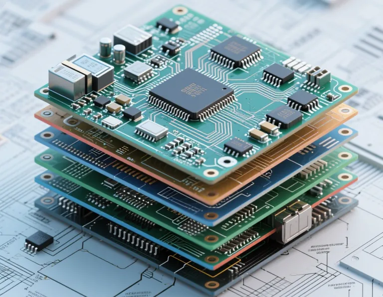
A single-layer PCB has limited routing options, while a double-layer PCB provides more flexibility. Most modern applications, however, use multi-layer PCBs, typically four or more layers.
A four-layer PCB usually includes a top layer, bottom layer, and two inner layers — one for power and one for ground — improving circuit performance, signal integrity, and electromagnetic compatibility.
Stack-up Design
Multi-layer PCBs are composed of alternating conductive and insulating layers. Conductive layers are made of copper, while insulation comes from prepreg and core materials.
A good stack-up design — such as dedicating inner layers for power and ground — reduces noise, improves shielding, and enhances overall reliability.
Key PCB Terminology
- Trace: Conductive path connecting pads and vias.
- Pad: Connection point for surface-mounted components.
- Through Hole: Hole for inserting leads or creating inter-layer connections.
- Via: Conductive hole used to route signals between layers.
- Mounting Hole: Mechanical hole for board fixation, non-electrical.
- Plane Layer: Large copper-filled area, often used for power or ground.
- Silkscreen Layer: Printed markings showing component labels and orientation.
Conclusion
The PCB is the foundation of all modern electronics, serving as both the physical and electrical backbone of devices.
From simple circuits to advanced multi-layer boards, PCB design determines the reliability, efficiency, and performance of every electronic product.