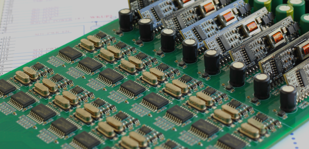
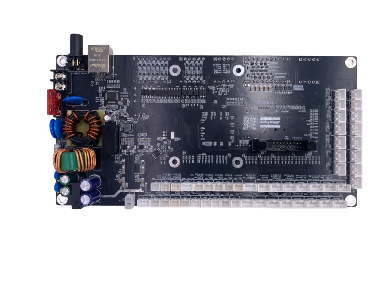
PCB (Printed Circuit Board), also known as a printed circuit board, is an important electronic component, a support for electronic components, and a carrier for the electrical connection of electronic components. Because it is made by electronic printing, it is called a “printed” circuit board. As electronic equipment becomes more and more complex, the requirements for PCB size are getting smaller and smaller. At the same time, the difficulty of PCB design is getting greater and greater. Today, this article will talk about several key points to grasp in an excellent PCB design.

PCB layout work is very boring in the eyes of many people, and even many engineers think so. Every day, they face thousands of lines on the board, various packages, and repeat the work of pulling wires. In fact, designers must take into account performance, cost, process and other aspects, and pay attention to the reasonable and neat layout of the board, so it is not as simple as it looks, and requires more wisdom.
Let’s talk about developing some good working habits during design, which will make your design more reasonable, easier to produce, and perform better. Before starting to design an excellent PCB work, you should carefully analyze the design and set up the tool software carefully, and do the following work.
1.Draw a good schematic diagram
Many engineers think that layout work is more important. The schematic diagram is used to generate a netlist for PCB inspection. In fact, the schematic diagram will play a greater role in the subsequent circuit debugging process. Whether it is to find problems or communicate with colleagues, the schematic diagram is more intuitive and convenient. In addition, develop the habit of marking in the schematic diagram, marking the problems that need to be paid attention to when laying out each part of the circuit on the schematic diagram, which is a good reminder for yourself or others. Hierarchical schematic diagrams divide circuits with different functions and modules into different pages so that the workload can be significantly reduced, whether reading the diagram or reusing it in the future. Using a mature design is always less risky than designing a new circuit. Every time I see all the circuits put on a drawing, a densely packed device, my head will be enlarged.
2.Good circuit layout skills
After the impatient engineer draws the schematic and imports the netlist into the PCB, he can’t wait to put the components in place and start pulling wires. In fact, a good PCB layout can make your subsequent pulling work easier and make your PCB work better. Each board will have a signal path, and the PCB layout should also try to follow this signal path so that the signal can be transmitted smoothly on the board. People don’t like to walk through a maze, and the same is true for signals. If the schematic is designed according to the module, the PCB can be the same. The board can be divided into several areas according to different functional modules. Separate analog and digital, separate power signals, separate heat-generating devices and sensitive devices, do not put large devices too close to the edge of the board, pay attention to the shielding of RF signals, etc. Spend a little more time optimizing the PCB layout, and you can save more time when pulling wires.
3.Learn to set rules
In fact, now not only does advanced PCB design software need to set wiring rules, but some simple and easy-to-use PCB tools can also set rules. After all, the human brain is not a machine, so it is inevitable that there will be negligence and mistakes. Therefore, we set some easily overlooked problems into the rules, let the computer help us check, and try to avoid making some low-level mistakes.
In addition, perfect rule settings can better standardize the subsequent work. As the saying goes, sharpening the knife does not delay the chopping of wood. The more complex the scale of the board, the more important the rule setting is. When the signals or power supplies between the interconnected PCB boards are in action, for example, when the power supply or signal of board A is sent to board B, there must be an equal amount of current flowing back from the ground layer to board A. The current on the ground layer will flow back to the place with the lowest impedance. Therefore, at each interface where the power supply or signal is connected, the number of pins allocated to the ground layer should not be too small to reduce the impedance, so as to reduce the noise on the ground layer. In addition, the entire current loop can also be analyzed, especially the part with larger current, and the connection method of the ground layer or ground wire can be adjusted to control the flow of current and reduce the impact on other, more sensitive signals.
4.PCB wiring technology
Whether to use a double-sided board or a multilayer board when making PCBs depends on the highest operating frequency, the complexity of the circuit system and the requirements for assembly density. When the clock frequency exceeds 200MHZ, it is best to use a multilayer board.
If the operating frequency exceeds 350MHz, it is best to use a printed circuit board with polytetrafluoroethylene as the dielectric layer, because its high-frequency attenuation is smaller, the parasitic capacitance is smaller, the transmission speed is faster, and the power consumption is reduced due to the larger Z0. The following principles are required for the routing of the printed circuit board:
1) All parallel signal lines should be spaced as far as possible to reduce crosstalk.
If there are two signal lines that are close to each other, it is best to run a ground wire between the two lines, which can play a shielding role.
2) When designing signal transmission lines, avoid sharp turns to prevent sudden changes in the characteristic impedance of the transmission line and reflection. Try to design it into a uniform arc line with a certain size.
3) The width of the printed line can be calculated according to the above-mentioned characteristic impedance calculation formula of microstrip line and strip line. The characteristic impedance of the microstrip line on the printed circuit board is generally between 50 and 120Ω. In order to obtain a large characteristic impedance, the line width must be made very narrow. But very thin lines are not easy to make.
Considering various factors, it is generally more appropriate to choose an impedance value of about 68Ω, because choosing a characteristic impedance of 68Ω can achieve the best balance between delay time and power consumption. A 50Ω transmission line will consume more power; a larger impedance can certainly reduce power consumption, but it will increase the transmission delay time.
Since the negative line capacitance will cause the transmission delay time to increase and the characteristic impedance to decrease, the intrinsic capacitance per unit length of the line segment with very low characteristic impedance is relatively large, so the transmission delay time and characteristic impedance are less affected by the load capacitance.
An important feature of a properly terminated transmission line is that the branch short line should have little effect on the line delay time. When Z0 is 50Ω, the length of the branch short line must be limited to within 2.5cm to avoid large ringing.
4) For double-sided boards (or four-layer lines in a six-layer board), the lines on both sides of the circuit board should be perpendicular to each other to prevent mutual induction and crosstalk.
5) If there are high-current devices on the printed circuit board, such as relays, indicator lights, speakers, etc., their ground lines should be separated and routed separately to reduce noise on the ground lines. The ground lines of these high-current devices should be connected to an independent ground bus on the plug-in board and the backplane, and these independent ground lines should also be connected to the ground point of the entire system.
6) If there is a small signal amplifier on the board, the weak signal line before amplification should be kept away from the strong signal line, and the routing should be as short as possible, and if possible, it should be shielded with a ground wire.
5.The more you consider others, the less work you do?
When designing PCBs, try to consider the needs of the end users. For example, if you are designing a development board, you should consider placing more silkscreen information when designing the PCB, so that it will be more convenient when using it, and you don’t have to look up the schematic or find the designer for support.
If you are designing a mass-produced product, you should consider more problems that will be encountered on the production line, such as the same direction of the same type of devices, whether the device spacing is appropriate, the width of the process edge of the board, etc. The earlier these problems are considered, the less they will affect the subsequent design, and the workload of the subsequent support and the number of board changes can also be reduced. It seems that the time spent on the initial design has increased, but in fact, it has reduced your subsequent workload. When the board space signal allows, try to place more test points to improve the testability of the board, so that you can also save more time in the subsequent debugging stage and provide more ideas for finding problems.
6.Do details determine success or failure?
PCB design is a meticulous job that requires carefulness and patience. The mistakes that novices who are just starting to design often make are some details. The device pins are wrong, the device package is used incorrectly, the pin order is drawn in reverse, etc. Flying wires can solve some of them, and some may turn a board into waste. Check it more when drawing the package, print out the package and compare it with the actual device before submitting the board. It is not obsessive-compulsive disorder to take a closer look and check it more. It is just to avoid these low-level mistakes that are easy to make. Otherwise, no matter how beautiful the design is, it is full of flying wires, which is far from being excellent.
7.Try to do a simulation?
Simulation is often something that PCB design engineers are reluctant to touch. Some people may say that even if I simulate, there will still be a difference between the actual PCB and the simulation result, so why should I waste time on simulation? Doesn’t the board I made without simulation work well? I am helpless with this idea. There is no problem with one or two designs, but it does not mean that there will be no problems in the future.
Although there are differences between the simulation results and the actual results, the simulation can show the correct trend of change, and we can make our own judgments based on the trend. It may be difficult at the beginning, and it is normal to be confused about the simulation parameters and simulation models. As long as you start, do it slowly, and accumulate experience slowly, you will realize the importance of simulation. Before the board is completed, you can determine the location where problems are likely to occur in advance, solve them in advance, and avoid problems. The more simulations you do, the more you will understand the causes of the problems, which will be of great help in improving your design capabilities.


