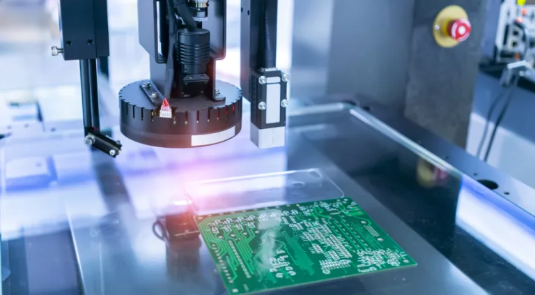

For hardware engineers, PCB design directly determines the performance and long-term reliability of electronic devices. Among all design considerations, PCB thermal design is often overlooked but plays a critical role in preventing performance degradation, instability, or permanent damage.
This article provides a complete, engineering-oriented overview of PCB thermal design — including layout optimization, component-level heat dissipation, board-level cooling strategies, and thermal resistance analysis — helping you build robust and reliable hardware systems.
Layout Design: The Foundation of PCB Thermal Design
Thermal management begins with proper component placement. A well-designed layout can significantly reduce junction temperature and improve system reliability.
1. Place high-power components in areas with good airflow
- Near PCB edges, air inlets, or regions with higher airflow
- Use CFD simulation to analyze airflow patterns in different layouts
2. Maintain sufficient spacing between heat-generating components
- Prevent heat accumulation
- Spread heat evenly across the PCB surface
3. Keep temperature-sensitive components away from hot zones
Typical sensitive components: oscillators, memory, MCUs, CPUs
Guidelines:
- Natural convection (sealed case): place sensitive components at the bottom
- Natural convection (unsealed): near air inlet
- Forced air cooling: in the airflow inlet zone
4. Use airflow distribution to optimize placement
- High-velocity airflow areas are ideal for high-power components
- Avoid large empty regions along airflow paths
5. Stagger heat-generating components along airflow direction
- Reduce thermal stacking
- Avoid downstream components overheating due to airflow shadowing
6. Consider the influence of heat sinks
Heat sink bypass airflow may:
- Increase heat transfer of side components
- Strengthen or weaken cooling of downstream components → requires monitoring
Thermal Design for Different Component Packages
Each package type has a different heat path, so thermal design must be package-specific.
1. THD components
- Limited thermal conduction to PCB
- Mainly rely on surface convection → Focus on airflow enhancement
2. SMD components
- Strong thermal coupling with PCB
- PCB becomes a major heat path → Central consideration in PCB thermal design
Enhancement strategies include:
- Thermal pads
- Large copper areas
- Thermal via arrays
3. PGA / BGA
- Used in CPUs, GPUs, ASICs
- Rely on heat sinks + thermal interface materials + forced air cooling
Practical Case
A thermal model mismatch in TIM thickness (0.3 mm vs. Intel’s 0.13 mm) caused a 20°C difference in CPU junction temperature.
→ TIM thickness is a critical parameter in PCB thermal design.
PCB-Level Heat Dissipation Techniques
1. Large copper pours
- Larger copper area = lower junction temperature
- Suitable for MOSFETs, DCDC modules, power ICs
2. Thermal vias
Benefits:
- Improve vertical heat transfer
- Provide heat path to the back of the PCB
Simulation shows:
- 6×6 thermal vias reduce junction temperature by 4.8°C
- Reducing to 4×4 increases temperature by ~2.2°C
3. Exposed copper on IC bottom pads
- Reduces air-interface thermal resistance
- Works best with surface treatment and coatings
4. Follow IPC-2221B guidelines
Ensure thermal design does not compromise electrical or mechanical performance.
Thermal Resistance Analysis
Thermal conduction can be compared to electrical conduction:
- Temperature difference ↔ Voltage
- Heat transfer ↔ Current
- Thermal resistance ↔ Electrical resistance
Key parameters
- Rjc: Junction-to-case resistance
- Rja: Junction-to-ambient resistance
- Conduction resistance: δ/(λA)
- Convection resistance: 1/(αA)
Contact thermal resistance
- Caused by micro-air gaps between two surfaces
- Reduced by higher pressure or thermal interface materials (TIMs)
Improvements
- Selecting proper TIM materials
- Optimizing TIM thickness
- Increasing airflow
- Using larger or more efficient heat sinks
- Reducing power consumption of the source device
Conclusion
PCB thermal design is a multi-disciplinary engineering process requiring careful balancing of layout, copper distribution, thermal vias, package thermal characteristics, and industry standards.
With extensive real-world experience in PCB thermal design, RF pcb design, EMC, and high-speed layout, Tronixv provides professional hardware development services that ensure reliability even under extreme operating conditions Contact us.