EMC on printed circuit boards is a common pain point for hardware engineers. Questions frequently arise: how should the PCB stackup design be arranged to minimize radiation and interference? Do EMC priorities change with different layer counts? This guide compiles practical, engineering-driven advice on PCB EMC design — covering component placement, layer stack-up choices, routing and grounding techniques — so you can quickly identify risks and apply effective mitigation in real projects.
Component Layout in PCB EMC Design
In PCB EMC Design, three factors must be considered first: number of I/O pins, component density, and power consumption. A practical rule: chip components occupy about 20% of substrate area and power dissipation should stay below 2W per square inch.
1. Functional Zoning
- Place related components close together.
- Keep digital, analog and power circuits separated.
- Separate high-frequency and low-frequency circuits.
2. High-Frequency Component Placement
- Keep HF traces short to reduce parasitic parameters.
- Crystal oscillators must be close to the clock-receiving chip and away from interfaces and low-level signal devices.
3. Component Orientation & Vias
- Components should be placed parallel or perpendicular to edges to minimize parasitic effects.
- Power and ground pads should be symmetrically distributed.
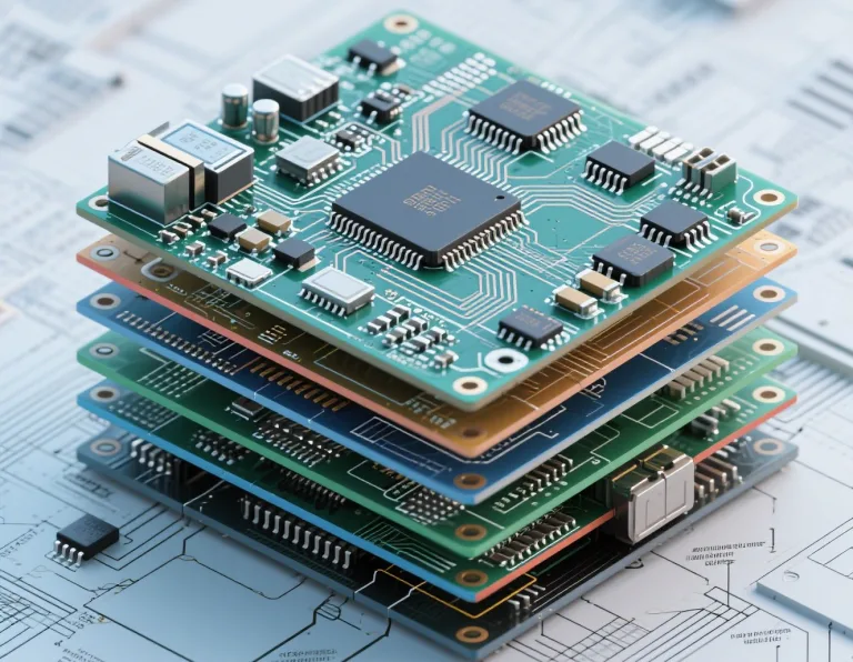
4. Multilayer PCB Layer Arrangement (Critical in PCB EMC Design)
- Place power and ground planes in inner layers as shielding.
- Ground plane above the power plane improves decoupling through interlayer capacitance.
- Signal layers should be arranged adjacent to ground/power planes.
PCB Routing Rules (Key to Effective PCB EMC Design)
Ignoring routing EMC factors may significantly increase EMI radiation. Good routing practice is essential to successful PCB EMC Design.
1. Ground Design (Most Important in PCB EMC Design)
- Use separate grounds for analog and digital circuits; connect only at the power entry.
- Enlarge common ground traces or use a full ground plane to reduce loop area.
- Avoid comb-shaped ground structures.
- Use closed ground loops on multi-chip boards to enhance noise immunity.
2. Power Routing (High Impact on PCB EMC Design)
- Power traces should run close to ground to minimize loop area and reduce differential-mode radiation.
- Keep analog and digital power isolated in multilayer boards.
- Power planes should be adjacent to ground planes for shielding.
- Place decoupling capacitors close to chip power pins.
3. Signal Routing (Critical for Signal Integrity & EMC in PCB Design)
General Rules
- Key signals should route close to their return paths to minimize loop area.
- Sensitive low-level signals must not run parallel to high-current or high-voltage traces.
- Use stripline where possible; avoid layer transitions for high-speed signals.
- Maintain proper spacing between signal groups and insert ground shielding traces if needed.
Crosstalk Prevention
- Increase spacing and shorten parallel trace lengths.
- Avoid routing high-speed signals near PCB edges to prevent edge radiation.
4. Clock Circuit EMC Design
Clock circuits are major EMI sources. A 2ns rise-time clock may radiate up to 160MHz. Key EMC rules:
- Use star-shaped clock routing instead of daisy-chain.
- Keep oscillator input/output traces short.
- Clock capacitor ground traces should be wide and short.
- Minimize vias near the crystal oscillator.
Process & Component Selection in PCB EMC Design
1. Manufacturing Process
- Thin-film process: high precision, good for high-frequency, single-layer only, higher cost.
- Multilayer thick-film process: cost-effective and improves EMC by providing dedicated power/ground layers.
- LTCC (co-fired ceramic): supports more layers, embedded components, excellent for high-frequency and high-speed requirements.
2. Component Selection (Enhances PCB EMC Design Effectiveness)
- Prefer bare chips or SMD components for better EMC performance.
- Use lower-speed clock chips when possible.
- Avoid unnecessarily fast logic families (avoid AC if HC is sufficient).
- Capacitors should have low ESR to avoid excessive attenuation.
3. Package Selection
Metal-sealed packages (e.g., Kovar) provide strong shielding in EMC-sensitive environments.
Tronixv has years of extensive experience in covering high-speed, signal integrity, and electromagnetic compatibility challenges. We have delivered efficient and reliable solutions to numerous clients.Explore our case studies to see our successful projects, or contact us anytime for professional consultation and customized services.


