What gives you the biggest headache every time you design a PCB? Is it the dense alignment? Or make people crazy about EMI problems? The root of the problem may be hidden in the place you cannot see—the PCB stacked structure. When you design from the laboratory small batch to mass production, have you encountered a sudden deterioration of signal integrity? Did the PCB fail unexpectedly when the product’s operating temperature increased? These pain points are likely to originate from irrational stacked layer designs. As we face more and more high-speed circuit designs, reasonable stacking structure has become one of the key factors for the success or failure of the project.
Why is PCB stack-up design so critical?
When choosing a stacked-layer structure, you need to balance four key factors: product complexity, signal rate, EMC requirements, and cost budget. The following are the three core properties that it directly affects.
- Signal integrity: The integrity of the high-speed signal layer needs to be sandwiched between the power or ground plane, forming a stripline structure. For example, when layer 3 is used as a high-speed signal layer, the ground plane needs to be set up above and below.
- Electromagnetic compatibility (EMC): A reasonable stacking structure can reduce crosstalk by more than 60%. Multiple ground plane layers can effectively reduce the PCB board impedance and reduce common mode EMI.
- Mechanical stability of the stacked layers must be maintained symmetrically; otherwise, the difference between thermal expansion and contraction will make the board into a “curved screen,” and welding yield will plummet.
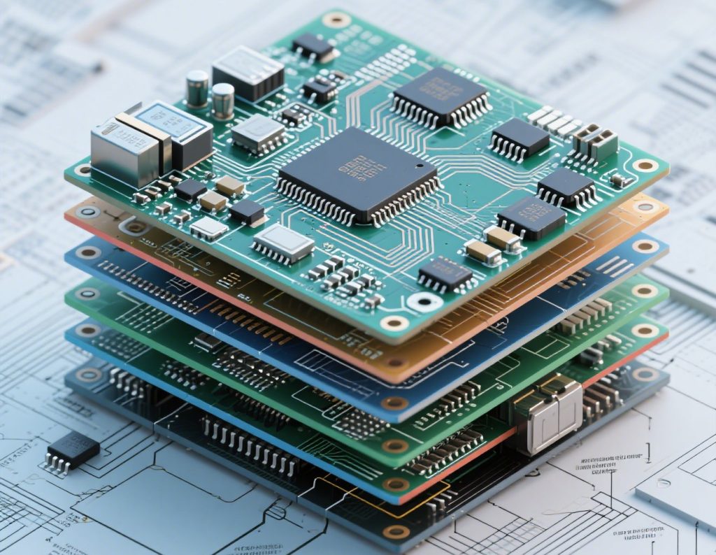
Different application scenarios of PCB stacking program selection
Double-layer board:
The cost of low-cost programs for simple structure and low signal rate applications, such as appliance controllers and LED driver boards. The cost advantage is obvious, but the EMC performance is poor, the signal is susceptible to interference, and it is not suitable for complex wiring. Design Tip: Try to increase the area of the ground as much as possible, where space allows, to form a local reference plane.
Four-layer board:
A cost-effective choice for common MCU development boards, industrial control boards, and other medium-complexity applications, a four-layer board is the best choice. Classic structure: TOP (signal) – GND – PWR – BOTTOM (signal). The advantage is that the signal layer is close to the reference ground layer, which can effectively control the impedance and reduce the signal return path length. Suitable for digital circuit design with differential signals or higher frequency. Advanced tips: The power supply layer adjacent to the ground layer controls the thickness of the interlayer medium in 0.1-0.2 mm and can reduce the power plane impedance.
Six-layer board:
A haven for high-speed signals. When encountering more high-speed signals (such as DDR4 and PCIe) or small board sizes and high wiring density, a six-layer board is a better choice. Recommended Architecture: TOP-GND-Signal1-PWR-GND-Signal2-BOTTOM This architecture sandwiches the high-speed signal layer (Signal1) between two ground planes for the best EMI suppression. Cost warning: for each additional layer, the cost may rise by 50%, but the EMI risk can be reduced by 30%.
Eight layers and above:
The ultimate in high-density design for high-complexity BGA packages or ultra-high-speed systems. Typical scheme: TOP-GND-Signal1-PWR-GND-Signal2-PWR-BOTTOM, four-layer signal, and the four-layer reference plane.
PCB stack-up design: five golden rules
Signal and power integrity priority high-speed signal layer:
Priority is laid in the inner layer of the ribbon line, from the reference plane ≤ 4 mil reference plane principle, to avoid the signal across the plane division area, otherwise leading to the return path breakage differential pair processing. Must be the same layer wiring, length deviation ≤ 5 mils, to avoid longitudinal broadside coupling.
Symmetrical design to eliminate stress, copper thickness, and mirror symmetry:
Such as the L2/L3 layer, are used. 1 oz. Copper foil media symmetrical distribution: the upper and lower half of the media thickness is the same. Special treatment: thick copper layer (≥ 2 oz.); adjacent layers need to be compensated for the design—every increase of 1 oz. of copper thickness, each side of the additional 1 PP.
Material selection determines the upper limit of performance:
For automotive electronics and other harsh environments, the choice of Tg ≥ 180 ℃ material so that the PCB in -40 ℃ ~ 150 ℃ temperature cycle under the reliability to enhance 30%+
Impedance control is the lifeblood of high-speed design:
- Accuracy control: the use of UV laser direct imaging (LDI) technology, line width tolerance ± 0.2 mil.
- Manufacturing Compensation: 1 oz. Copper thickness is actually counted in the model according to the 1.2 mil.
- Special plate: Rogers and FR4 mixed pressure, symmetrical position using the same coefficient of thermal expansion material.
Manufacturability design to avoid rollover:
PP sheet selection: no more than 3 sheets of PP media per layer. Stacking thickness control: PP media thickness between the two layers ≤ 21 mils (too thick leads to processing difficulties). Copper foil selection: preferably 0.5 oz. 5 oz copper foil for the outer layer and 1 oz for the inner layer; the power supply layer is selected according to the demand for current (2-3 oz).
Practical skills in the manufacturing process
- Foil vs. Core stacking method Foil method (outer layer pressed copper foil): low cost, but impedance control is difficult (surface layer flow problem). Core method (outer layer with core board): 20% higher cost, but high impedance precision.
- Mixed material pressing Rogers and FR4 mixed pressure; they need to use a stepped pressing process to prevent interlayer slippage.
- Thick copper plate manufacturing: more than 3 oz. Copper layer using a differential etching process—the first etching to 2 oz., the second graphic to the target thickness.
Design completion of the key step: using tools to verify the stacked layer
How to verify the stacked layer design after completion? Traditional methods rely on engineers’ experience; now, TronixV provides a one-stop solution.
Impedance Magic combines various production factors and automatically calculates or back-calculates impedance to ensure that impedance tolerance is controlled at ±10%.
OneOne-key analysis automatically detects hidden design problems, eliminates production difficulties and design defects, and warns of price-affecting factors.
Stacking Stacking verification software can automatically match the stacking structure in line with the production to ensure the reliable quality of multilayer PCB boards.
File comparison: Easily compare the differences between the before and after versions of the stacked layer to avoid human negligence.
Design tips: In advance of the simulation, you can find 80% of the signal integrity problems. Combined with TronixV’s manufacturing analysis, hidden problems can be solved before production.