When a peak voltage is input, there is a potential risk of IC pins being damaged. Peak voltage often comes from the superposition of reverse electromotive force pulses generated by ESD, hot swapping, and inductive load disconnection.
To prevent potential damage to the components in the circuit caused by spikes, TVS bypass is commonly used to discharge to ground, or a current-limiting resistor is used online to limit the surge of spike voltage into the IO port of the chip.
But TVS has three issues:
Firstly, TVS has a lifespan and is prone to damage due to aging over time;
The second is that TVS has a junction capacitor Cj. When using TVS bypass discharge on high-speed signal lines, there is a side effect. Due to the charging and discharging of Cj, there is a delay in the rising and falling edges of normal high-speed square wave signals, causing the square wave signal to start discharging on the falling edge before it reaches the high-level critical value, which limits the data rate.
The third is to spend money, especially for price-sensitive consumer electronics products.
There is an improved method that can be used for reference. Although it is not perfect, it can be considered as an additional optional solution that can effectively avoid the above disadvantages, which is the use of discharge teeth implemented on the PCB board through wiring.
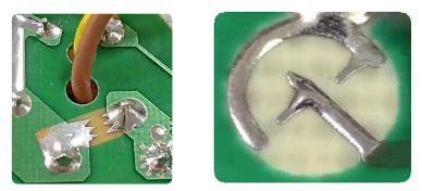
Add discharge teeth as shown in the figure at the static source end and the discharge end. The requirement for the discharge teeth is that the peaks are opposite, and there must be no solder mask layer (cut) on them. The tooth spacing between the tips is 1mm. The design basis for the 1mm spacing comes from two sources:
One is that the air breakdown field strength in dry air is 3 * 106V/m. When the ESD voltage is 3000V, with a spacing of 1mm, the 3000V peak just reaches the critical field strength for breakdown discharge; ESD of no less than 3kV can be released.
Secondly, considering the safety regulations, insulation and voltage withstand tests are generally conducted between 1500-2000V, and the discharge tooth gap must also ensure that no breakdown or conduction occurs during the voltage withstand test. So, the spacing between the discharge teeth is selected to be 1mm.
However, there is also a disadvantage to the discharge teeth, which is that with more discharge cycles, more carbon deposits will form between the teeth, which can easily lead to a decrease in the insulation impedance between the teeth, especially in humid and moisture-absorbing situations. It needs to be cleaned up in a timely manner. In situations where static electricity occurs frequently, use it leisurely.
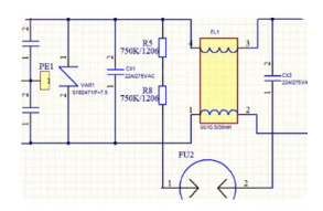
Discharge teeth are often added at both ends of the common mode inductor used to suppress surges in power or signal lines, to avoid the formation of a large voltage difference between the front and rear ends of the common mode inductor when the surge voltage is too high, thereby breaking through the insulation paint layer of the inductor coil winding.