
Introduction
Printed Circuit Boards (PCBs) are the foundation of modern electronics. From smartphones to industrial control systems, reliable PCB design and production are essential for stable device performance. This guide provides a full overview of the PCB development process—from manufacturing and assembly to testing and debugging.
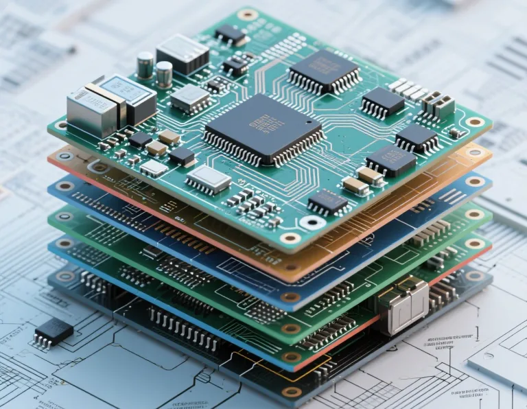
1. PCB Manufacturing Process
PCB manufacturing involves several precise steps:
- Design Using professional CAD tools (e.g., Altium Designer, Cadence Allegro, KiCad) to create schematics, layouts, and Gerber files.
- Etching UV exposure and chemical etching define the copper traces on the board.
- Drilling & Plating Holes are drilled for vias and component leads, then plated with copper for conductivity.
- Solder Mask & Silkscreen Protective solder mask prevents shorts; silkscreen printing adds labels and component identifiers.
Accurate Gerber files and manufacturing drawings ensure reliable and repeatable PCB production.
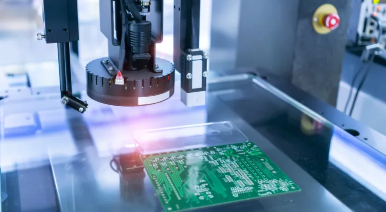
2. PCB Assembly Techniques
There are two primary assembly methods:
- Through-Hole Technology (THT) Ideal for components requiring mechanical stability or higher power dissipation.
- Surface Mount Technology (SMT) Enables compact, high-density designs suitable for automated pick-and-place machines.
Efficient assembly depends on proper component placement, clear documentation, and optimized soldering processes.
3. PCB Testing and Debugging
Testing ensures that every board performs as intended. Common methods include:
- Visual & AOI Inspection – Detect missing or misaligned components.
- In-Circuit Testing (ICT) – Uses bed-of-nails fixtures for electrical validation.
- Boundary Scan (JTAG) – Tests interconnections in dense PCBs.
- Functional & Thermal Testing – Validates performance under operational conditions.
Debugging tools such as oscilloscopes, logic analyzers, and thermal cameras help engineers quickly locate and correct issues.
4. Advanced PCB Design Techniques
Modern PCB design must address signal integrity, power integrity, EMC, and manufacturability:
- High-Speed Design – Controlled impedance routing, length matching, and differential signaling reduce reflection and noise.
- RF & Mixed-Signal Design – Separate analog/digital grounds, apply shielding, and use microstrip/stripline routing to minimize crosstalk.
- Emerging Trends – Integration of high-frequency laminates, embedded components, and additive manufacturing for next-gen designs.
5. Conclusion
Designing a reliable PCB requires expertise across every stage—concept, layout, assembly, and testing.
By adhering to best practices, maintaining thorough documentation, and leveraging advanced design tools, engineers can ensure both performance and manufacturability.
Continuous innovation in PCB design is essential for meeting the demands of modern electronic systems.