1. What Is a Low-Background PCB, and Why Does It Matter?
In the context of advanced scientific research, “low background” refers to minimizing radiation originating from the intrinsic radioactivity of materials (e.g., trace isotopes from the U / Th decay chains, potassium, cobalt) as well as parasitic noise and background counts introduced by impurities, ionic residues, or surface contamination.
In rare-event detection (such as dark matter searches, neutrinoless double beta decay, low-energy neutrino experiments), ultra‑low signal measurements, radiometric background calibration, underground or space experiments, superconducting quantum systems, and high-sensitivity detector readout electronics, the mechanical and electrical support structures—including the PCB—can themselves become measurable sources of background. This elevates system noise floors, reduces sensitivity, or significantly extends the required integration time.
Therefore, a low-background PCB is not “just a normal board made with a different material.” Instead, it is the result of a closed-loop engineering methodology:
Material Selection → Design Strategy → Process Control → Cleaning & Testing → Supply Chain Traceability → Data-Driven Validation.
2. Project Background and Collaboration Value
This project originates from a frontier scientific research platform at a Top 10 domestic university. The research requirements simultaneously emphasize mechanical support for electronics, low-noise signal conditioning, power distribution integrity, and stringent control of material radioactivity. We have built a tailored process and quality validation framework around two core goals: low background and manufacturability (with scalability and iteration speed considered during planning).
3. Design: Balancing Electrical Performance and Background
Stack-Up Strategy
- Control total copper mass: Use thinner copper or patterned “copper relief” (mass reduction windows) in low-speed / low-current sections to reduce total material contributing to background.
- Power vs. analog isolation: Shorten the routing length of sensitive front-end analog paths to decrease dependence on large continuous ground copper planes.
- Minimized shielding mass: Where shielding is essential, adopt detachable external shield cans instead of permanently integrated heavy copper areas.
Vias and Metallization Control
- Optimize via density: Avoid habitual over‑drilling, which increases overall plated copper volume.
- Micro/blind vias in critical zones: Evaluate whether laser drilling residues and subsequent chemical treatments could introduce trace contaminants.
Functional Zoning
- Isolate high-sensitivity readout regions from clock/power domains to reduce electromagnetic interference and thermal noise—lowering the system’s effective background.
Manufacturability and Iteration
- Early co‑engineering with the fabrication house on feasible stack-up windows ensures alignment between low-background constraints and production capability, preventing repeated redesign cycles and delays.
4. Base Material
Why Not FR4?
Standard FR4 typically contains brominated flame retardants, glass fiber, fillers, and curing accelerators—each a potential carrier of trace U/Th/K or heavy metals.
Our Approach
Adopt specialized low-radioactivity polyimide or modified low‑filler epoxy systems as the PCB substrate for reduced intrinsic background.
5. Adhesives (Prepreg / Bonding Systems)
- Source Components of Concern: Resin, curing agents, accelerators, and mineral fillers may contain trace K, Ba, Sr, Pb, and U/Th.
- Selection Principles: Low ash content, halogen-free, and low metallic ion extraction values (post leach tests).
- (Optional for future detail: Batch screening via ICP-MS and ion chromatography for Na⁺ / K⁺ / Cl⁻ residues.)
6. Copper Foil
- Contamination Risk: Standard electrolytic copper can contain trace Co, Ni, Fe; downstream cleaning or anti-oxidation treatments may introduce Cl or Na.
- Solution: High-purity cathode copper (≥ 99.99%). Require suppliers to provide background characterization (U / Th / K) plus impurity spectra.
- Controlled handling: Dedicated clean cutting and nitrogen-sealed storage to minimize recontamination.
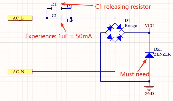
7. Soldering
- Use lead-free soldering processes with a no‑clean flux approach (provided flux chemistry is validated for low ionic and low radioactivity residue).
- If further background reduction is required, flux residue verification (ionic contamination, outgassing) can be added.
8. Cleaning
- Multi-stage ultrapure water cleaning; final drying under filtered nitrogen to avoid ionic redeposition.
- Ultrapure water resistivity control and periodic ion chromatography can be incorporated to verify consistency.